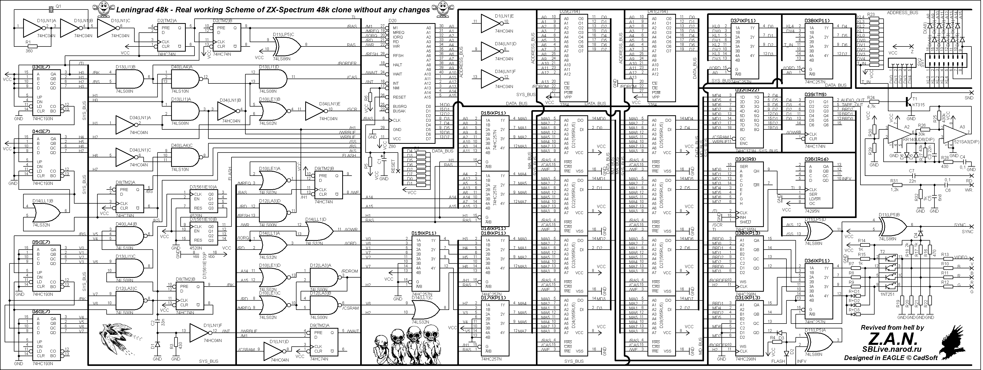
The Leningrad contains a shift register1, which I believe is loaded with data from the bitmap. This part loads 8 bits in parallel, and shifts each bit out in turn on the rising edge of a clock signal. This clock signal is called /ТИ (meaning Тактовый Импульс, or clock pulse, spelled TI in our alphabet) and is 7MHz (divided from 14 via a D flip flop).
Now, its output, a bitstream which makes up the picture, is fed to another shift register2. This one is a four-bit shift register, but only one bit is used. Its output is called INFV, which is fed to the demultiplexer that selects the attribute color. It's clocked to ТИ (the inverse of the signal which clocks the first shift register).
Why are two shift registers needed here? The four-bit one in particular makes no sense to me.
On the following schematic, this arrangement may be found on the far right, about half-way down. It's parts DD33 and DD35.

Edit: I have also seen variants using two ИР16s Iin place of the ИР9, three in total, possibly a BOM cost optimisation.
1: КР1533ИР9, or 74LS165, a parallel load 8-bit shift register
2: КР1533ИР16 or 74LS295, a 4-bit right-shift left-shift register with 3-state outputs