1

Let's say you have a hypothetical 8-bit processing machine with 256 bytes of memory. You want to load the value stored in memory location $f2 into a register.

However, with a data bus of just 8 bits, you can't use all of the memory unless you want to have no room left for an opcode. And having more than one operand would be impossible.

There are two solutions to this dilemma. The first solution is to increase the width of each memory location to 12 or 16 bits to have room for an opcode.

The second is what most computers use: multi-byte instructions. For example, an LDA instruction might have the opcode in one byte and the operand on a different byte following the first. However, this seems much more confusing to me. You have to fetch another byte while storing the first, which seems frankly impossible to me.

So how do computers execute multi-byte instructions and what are the microinstructions for such a Herculean task?
7
  • 4
    I'm guessing that if you think decoding and executing a multi-word instruction is fundamentally more difficult than decoding and executing a single-word instruction, then you probably haven't given a lot of thought to the sequences of things that a CPU must do to decode and execute many of the single-word ones. For the broadest of broad strokes, you might want to Google for information about "Sequential logic circuits." Commented May 28, 2020 at 13:11
  • But it is fundamentally more difficult. The CPU has to do another fetch cycle, which means resetting the control unit while storing the opcode an a register and then after that fetching the operand. Then the CPU must have a machine that knows when the fetching is going to stop and if this is sounding confusing then it is. A single byte instruction only requires you to fetch once every time, not some variable amount.
    – Nip Dip
    Commented May 28, 2020 at 15:01
  • 3
    I'm inclined to vote for colure, as this is not an RC specific question, but a general CS/EE one: How to design a (word) size CPU wit multi word instructions.
    – Raffzahn
    Commented May 28, 2020 at 15:41
  • @Raffzahn Yes. But it could be made on-topic if ask about a specific implementation. Commented May 28, 2020 at 15:42
  • 1
    @Wilson True. But his problem isn't how a specific CPU works, but the general working ... and to be honest, I have an ida were he's stuck, but that's again a generic design issue, nothing specific RC.
    – Raffzahn
    Commented May 28, 2020 at 15:44

3 Answers 3

4

[Preface: This question is independent of word size or CPU, and in no way RC.SE specific, but a basic lesson about processor design, so it might be more appropriate to ask in SO, CS or EE]

It's as simple as 1, 2, 3.

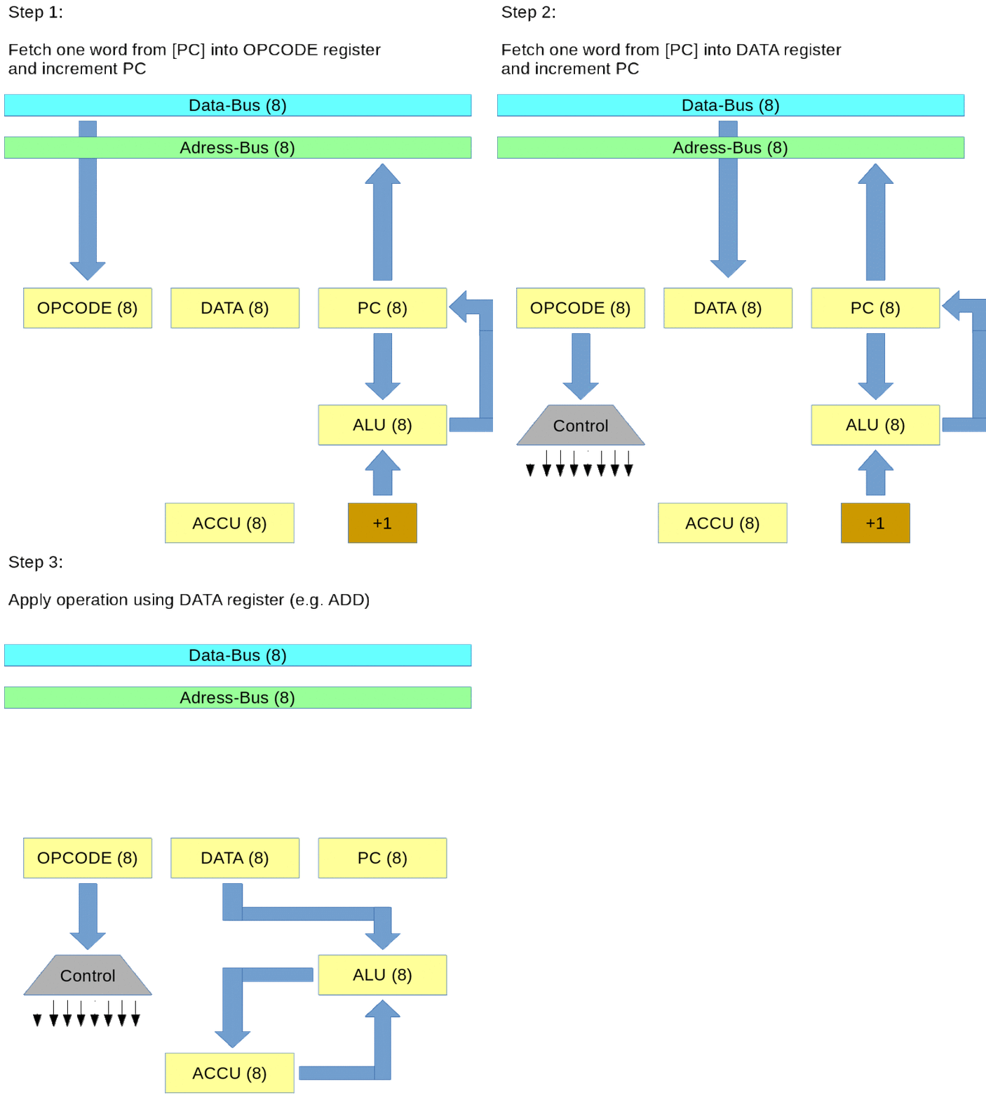
A two word immediate operation could run like this:

  1. Fetch one word from [PC] into OPCODE register and increment PC

    OPCODE-Register can now be decoded and act upon by

  2. Fetching one word from [PC] into DATA register and increment PC

  3. Apply operation using DATA register

The last step is whatever the operation read in step 2 commands:

  • If it's a LOAD ACCUMULATOR WITH IMMEDIATE VALUE than DATA gets moved into ACCUMULATOR.
  • If it's an ADD IMMEDIATE VALUE TO ACCUMULATOR, then DATA gets added to the ACCUMULATOR.
  • And so on ...

The operation to be sequenced will always be held in OPCODE during all steps, that is until finished and the next one is loaded. Thus OPCODE can always deliver the needed information to decode and operate.


Or as an animated GIF:

enter image description here

(And yes, there are possible optimisations and alike (And I'm not an artist at all), but that's not the point)

0
6

One example is the 6502. It fetches an opcode, and then while storing the opcode in internal memory, fetches some argument which may be 1 or 2 bytes. This is not hard to achieve, it is not a Herculean task.

While the instruction executes, the operand might be stored in another register, routed through the ALU or other circuitry, or whatever.

Another example is the Z80, which has multiple byte instructions. This works by having prefix bytes which I believe set some internal state which affects the decoding of the opcode proper.

6
  • 1
    Using little-endian addressing allows read instructions using the abs,x, abs,y, or (ind),y addressing modes to run a cycle faster in the non-page-crossing case than would be possible using big-endian.
    – supercat
    Commented May 28, 2020 at 17:46
  • @Almo: See comment above. Big-endian is more "human readable" because bytes are usually written with higher addresses on the right, but human-readable numbers are written with the upper digits on the left. For many processing tasks, however, little endian will be more efficient.
    – supercat
    Commented May 28, 2020 at 17:48
  • 1
    [in case anyone is curious, the advantage with little-endian on the 6502 is that the processor can compute the lower byte of the address while it's fetching the upper byte. If it fetched the upper byte first, it wouldn't be able to know whether to add 1 or not until after had not only fetched the lower byte, but added the index register to it. In fact, if using big-endian, unless one adds extra circuitry, the page-crossing penalty would apply in addition to the extra cycle needed to compute the lower byte.]
    – supercat
    Commented May 28, 2020 at 17:52
  • Ok I got them mixed up; been over 20 years since I did that stuff. I meant that it made me like little-endian, the way the 6502 does it! :D The labels seem backward to me; I'd expect big-endian to mean "big at the end".
    – Almo
    Commented May 28, 2020 at 17:53
  • 1
    @Almo Learning 68k assembly in the mid 80s made me hate x86!
    – Glen Yates
    Commented May 28, 2020 at 20:24
2

"You have to fetch another byte while storing the first, which seems frankly impossible to me."

In simple words CPU is storing first byte (opcode) in internal register(s). Most (or maybe all) CPUs are realized as finite-state machine (https://en.wikipedia.org/wiki/Finite-state_machine). Most known CPU states are FEtch, Instruction Decode, EXecute, MEMory access. Every instruction is processed in few internal steps (finite-state transitions).

4
  • Yeah, but the problem is that the CPU has to restart another fetch cycle, and then jump to the requested microcode to execute it. That seems very difficult to perform.
    – Nip Dip
    Commented May 28, 2020 at 14:59
  • I think you're mixing levels. An instruction is a computer program being executed by the microcode engine, which has its own fetch/execute cycles. Meanwhile there's a microprogram counter which is advancing sequentially through the microinstructions that are the microprogram for the instruction being executed.
    – dave
    Commented May 28, 2020 at 17:47
  • 6502 or other 8bit CPU from 80s has no microcode at all. As i sad, CPU i finite-state machine, it's steps from one state to other and it's rather simple idea. Initialy CPU is in state FETCH so CPU outputs reg PC on address bus, reads 1 byte, puts this byte in OPCODE reg and steps to DECODE state. In DECODE state CPU is processing data from OPCODE reg using logic hardcoded in hardware (binary gates connected by wires). For some opcodes next state would be EXECUTE for other it will be FETCH_SECOND_BYTE. There are many internal states in typical CPU.
    – ufok
    Commented May 29, 2020 at 5:44
  • @NipDip why does it seem difficult to perform? in a microcoded CPU, this could be done by the first byte jumping to microcode which does another fetch cycle Commented Dec 8, 2022 at 13:03

You must log in to answer this question.

Not the answer you're looking for? Browse other questions tagged .