12

I am creating a minimal Z80 computer with serial output on a breadboard. I have kind of moved up from the last question, where I was executing instructions on Z80 using specific connection of resistors on data bus. Now I am finally hooking up the Z80 with ROM and RAM chips. Many websites list that the maximum space that the Z80 itself can address is 64K (2^16). I have 32K SRAM chip and 32K EEPROM, so I want to add both chips to the 64K address space, it just fits to the limit, right? Would it be possible to fully operate with whole 32K RAM and 32K ROM without using manual bank selection to determine, which address space part should be used?

I was thinking about using 74HCT139 1 from 4 decoder. I want to divide 64K address space into four parts of 16K. So I will be able to use 14 address pins to address 16K and 2 address pins will be free to use in 74HCT139. Thanks to the decoder I will get 4 signals, which will help me to get into 1 of the 4 address spaces. For this case I would like to use OR gate like 74HCT32. Please see the image below, I tried to express myself through the picture. Each chip (ROM and RAM) has 2 address space parts, which means, that I will be fine using 0 or 1 to determine, which address space part is indeed.

So my question is:

Is my decoding logic valid?
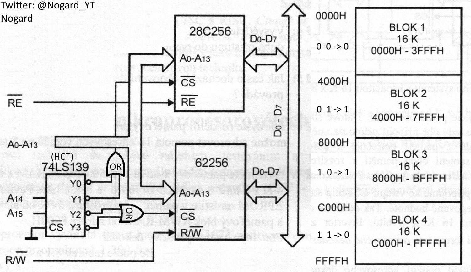
Logic scheme + address space

7
  • 12
    Why not simply route A15 to the chip-select pin of the 28C256 chip, and route NOT A15 to the other chip-select pin? Your chip selects do not appear to depend on A14 at all. Commented Apr 27, 2020 at 12:16
  • 4
    Doesn't those memory chips have a A14 line? Without that 32KByte is difficult to adress.
    – UncleBod
    Commented Apr 27, 2020 at 14:31
  • Are you sure the chips are 32 KByte? In memory chips, the usual measure is kilobits not bytes. (or nowadays gigabits instead of gigabytes.)
    – MSalters
    Commented Apr 28, 2020 at 9:50
  • A quick check on 28C256 indicates that it's 256Kbit, organized as 32Kx8, with 15 address lines (A0-A14). I would assume the RAM is organized the same way.
    – jeffB
    Commented Apr 29, 2020 at 14:18
  • What do you mean by "serial computer"? This doesn't look anything like the description at "serial computer".
    – David Cary
    Commented May 26, 2020 at 23:33

3 Answers 3

8

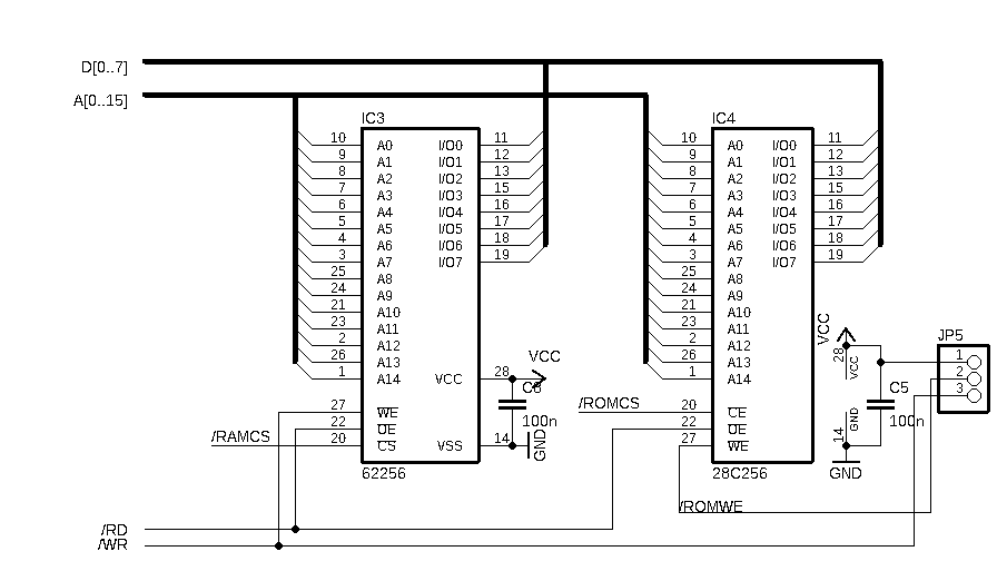
I have solved a similar problem when reworking my 8085-based OMEN Alpha computer for the Z80 CPU. The memory part is really simple:

OMEN Alpha Z80 Memory circuit

You have two memories, 32k each, and you should map the EEPROM from 0000h, RAM from 8000h. I use common data and address bus, as well as the control bus (/RD and /WR). The only memory-specific signals are /RAMCS and /ROMCS. They are generated by 74HCT00 chip this way:

OMEN Alpha Z80 Memory decoder

As you can see, all you need is the A15 (the highest) address signal, gated by /MREQ signal.

/ROMCS is active(=0) when /MREQ is active and A15=0, /RAMCS is active when /MREQ is active and A15=1

6
  • 1
    Yes, that's a nice, straight forward solution. A single simple '00 doing the job. Much like it was done back then.
    – Raffzahn
    Commented Apr 29, 2020 at 0:27
  • 1
    Thank you so much for the great answer, Martine. :) I read your book, you have my respect. The book "Porty, bajty, osmibity" is perfectly written.
    – Nogard
    Commented Apr 29, 2020 at 9:40
  • 2
    In some cases, it may be useful to design a system so that following a reset, all reads will be served by the ROM until some action occurs, and once that happens the lower part of the address space would be RAM and the upper part ROM. Code could then start by performing a jump to the upper part of the address space and enable RAM in the lower part. This would allow programs to set up RST vectors for quick little subroutines. Microsoft's original BASIC for the 8080 used some RST vectors for that purpose.
    – supercat
    Commented Apr 29, 2020 at 17:31
  • This is quite similar to what I did. On my design, though, by moving a couple of jumper wires, I can select anything from 2K of ROM to 32K of ROM, with the balance being RAM. But this design above is quite like mine in 32/32 mode. A15 is the only wire you need, as it splits the 64K into two parts.
    – TomServo
    Commented Jun 2, 2020 at 16:40
  • Aren't you forgetting about /RFSH? Or does your system have static RAM only? Commented May 7, 2022 at 10:58
13

Your observation about the 64K address space is correct, your 32K RAM and 32K EEPROM will be able to fill that address space to 100%. In Z80 designs, the ROM/PROM/EPROM/EEPROM is usually placed starting at 0x0000 since when you do a RESET, the Z80 starts executing at 0x0000 and you usually want to have your program start there.

Of course there are many variations on this depending on your application but this is probably a good place to start.

If you were merely using the two 32K devices as they are, you could use the A15 address line as your select between the two. A15 would be low for the first 32K of addresses and could serve as the chip select or /CS (normally an active low signal) and the inverse of A15, or /A15 could serve as the /CS for your RAM.

So all you'd need is an inverter such as a 74LS04 or similar. If you want to split into 4 spaces, a decoder such as the 74LS139 is a good choice and your logic looks ok to me.

0
10

Sure, it works, but then again, why decoding four 16 KiB blocks when it's about two 32 KiB chips? All you need to decode is A15.

  • A15=LOW should select the ROM (*1), while
  • A15=HIGH does the same for RAM

Inccoperating a A14 is rather pointless and using a'139 looks like overkill unless there is some future use. It also adds signal time, limiting maximum speed. Instead this might be done with a single NOT gate, like one element of a '19 (*2) put inbetween A15 and CE of the RAM, so way less effort.


(This might be already covered in missing parts of the schematic)

But more important then decoding is the way access is handled. For one, the Z80 does not supply any R/W signal like the for example Motorola, but separate signals for read (/RD) and write (/WR). Equally important, it provides a /MREQ signal marking memory access.

All three need to be incooperated to generate the needed /CS, /OE and /WR (*3) for either chip.


*1 - x80 type CPU need ROM on address zero for the reset vector

*2 - Or one element of an all ubiquitous 7400 NAND with both inputs connected. On a 74xx design there's are always at least one left :)

*3 - In fact, since you're using an EEPROM, /WR can be generated for both to allow in system updates ... maybe with a security switch to disable this during non update times :)

You must log in to answer this question.

Not the answer you're looking for? Browse other questions tagged .