36

Intel has named the i7-8086K in honor of the 8086 processor, though itself it is a 64-bit processor. And we still see in embedded systems or MIL-SPEC platforms there are old CPUs like the 80386 produced in the original, say, 1 µm process. However, is there any CPU produced in, say, 14 nm process, but with as few transistors as the original 8086 or 80386 (which Linux dropped support for and moved on to the 80486 for some reason I've no idea of), etc. – thus useful enough for certain purposes, but faster than the original ones while cheaper and cooler than modern CPUs?

Edit Jan. 2023: Garth Wilson quoted an interview of Bill Mensch on the 6502 and '816 in Nov. 2015.

He figures that if they went to 20nm geometry for the 65c02 like the newest Intel processors use, and put the memory and I/O onboard, they should be able to run at 10GHz. [Edit, Oct 2022: Now they're down below 5nm! What would that do to the speed?]

Steve Furber, a former Acorn engineer, claims in a speech on 06/07/2013 that SpiNNaker, a massively parallel system, would have 1 million processors work together the next year.

11
  • 23
    It’s just a tangential remark, but this is the commit that removed 386 support in Linux. The rationale was simply that working around old CPU bugs and lack of support for certain atomic instructions wasn’t worth the maintenance cost. Commented Mar 9, 2021 at 5:50
  • 2
    @user3840170 I was aware of the commit and related RC threads retrocomputing.stackexchange.com/q/194 and retrocomputing.stackexchange.com/q/1811, however to my limited knowledge I just cannot see where 80486 differs from 80386 apart from some extra onboard cache and related flushing instructions, and why it would make i386-compatibility unworthy.
    – Schezuk
    Commented Mar 9, 2021 at 6:13
  • 9
    For one, 80386 doesn't have cmpxchg instruction. You can even get the hint about this in the commit itself right at the beginning: - select HAVE_CMPXCHG_LOCAL if !M386.
    – Ruslan
    Commented Mar 9, 2021 at 15:28
  • 9
    hmm. I'd consider x86[-64] to be an outdated architecture lol
    – 12Me21
    Commented Mar 9, 2021 at 23:04
  • 6
    And, of course, the irony is that booting up a modern OS on that fancy new i7-8086K takes many times longer than booting up DOS or CP/M on the original 8086. Ah, "progress". Commented Mar 10, 2021 at 19:42

8 Answers 8

57

Manufacturing simple processors on newer semiconductor processes is done. But not quite to that extreme.

Let's consider your proposed 8086 done in a 14 nm process. Let's say we do it in CMOS, and maybe even throw in a few extra features, and it takes 100,000 transistors. The die would be very tiny, so unbelievably tiny. You could fit three thousand of them, with room to spare, in a single square millimetre, which is an area likely smaller than the period at the end of this sentence.

As you might already be imagining, slicing up, wiring up and packaging wafers with literally hundreds of thousands or millions of microscopic ICs is not very convenient. Using that old 180 nm fab, which costs far less to run too, starts looking attractive!

With that said, there is a market for simpler processors on something like a 180, 90 or 45 nm fab, which are still quite new compared to the 1000 nm in use at the time of the 80386. Consider all the microcontrollers. Very small 8-bit devices are still manufactured today, typically with transistor budgets in the ~100K - 10M range, including onboard RAM and peripherals and so on.

If you go a little bigger than that, the ARM Cortex-M devices, meant for embedded applications, are in the style of more traditional RISC processors of the 90s, and lack features we've taken for granted on desktops and servers for a while now, like single-cycle multiply instructions, virtual memory, or floating point; the smallest M0 cores are probably only about twice as complex, by gate count, as the original ARM processor from 1985.

One exception where you might actually implement such a device on a new process is when you want or need the power saving advantage. Due to the practicalities of how small a die can be as mentioned above, you basically have a free transistor budget up to a certain point after your main features are implemented. So you just spend like a drunken sailor. There is no manufacturing cost, or power drawback, to implementing features and just turning them off if you don't use them. That's part of why even the cheapest microcontrollers today usually have numerous onboard peripherals.

9
  • 13
    A period is one pixel on my 1080p 22", so you'd need a screen a metre high for it to be 1mm², or be viewing at 4x zoom. Commented Mar 9, 2021 at 13:29
  • 10
    @PeteKirkham It's 4 pixels on mine, so for me that period is about 1470 dies (or 0.49mm²). It's the right order of magnitude at least ;)
    – marcelm
    Commented Mar 9, 2021 at 17:05
  • 2
    @marcelm well, 0.49 is just not the same order of magnitude any longer (factor 0-5 - 5.0). But I appreciate the point, quite literally. Commented Mar 9, 2021 at 23:12
  • 2
    Many Cortex-M chips do have single-cycle multiply
    – scruss
    Commented Mar 9, 2021 at 23:47
  • 5
    It should also be noted that chip fabs are notoriously busy, and very capital intensive. Unless there's a huge increase in yield or production efficiency, keeping the old fabs around for work they're better at is a no-brainer. For the 8086, the die pictures at righto.com/2020/06/die-shrink-how-intel-scaled-down-8086.html show very nicely how much you could shrink the die - they already did, and the wiring is already as tight as it can be, more or less.
    – Luaan
    Commented Mar 11, 2021 at 7:09
48

TL;DR:

Older CPUs have been shrunk to smaller sizes but not in the same way as modern design, simply as there is no gain in doing so.


Details:

Does the industry continue to produce outdated architecture CPUs with leading-edge process?

No. Designs shrink, but there is no sense in using leading-edge sizes for such 'small' designs.

However, is there any CPU produced in, say, 14 nm process, but with as few transistors as the original 8086 or 80386

No, as these designs simply have gate counts that are too small to make it worthwhile. A 386 has at least 132 pins, each needing a pad on the die to connect to. With actual bonding technology a pad needs about 100-150µm, so 132 pads will take some 16mm (rounded for simplicity), making the chip at least 4x4 mm in size - or more precisely, that'll be the inner size available to its circuitry. That's a full 16mm². Using 12nm process that's enough for more than 200-300 million transistors, but an 80386 has under 300 thousand. It'll fit in 1000 times. Heck, even throwing in a 387 as well wouldn't change it much. No need to take on all the disadvantages of small node size without any gain.


The Long Read

Scruss's answer about the greatly revamped 8051 isn't wrong - the 8051 ISA is still a major seller in micro controllers, not least due to quite mature tools being available for them. But at the same time, these new 8051's have about as much in common with the original Intel CPU as a i7 has in common with an 8086. Yes, it has a mode to run the same code, but everything else is as different as it can get. Like apples and oranges.

The same goes for all examples involving ARM. True, a Cortex something (ARMv7/8) can run most code from an ARM 6 (ARMv3), but its inner workings and structure are different in almost all aspects.

But there are several real old CPUs that are still in production today, using the same internal structure, only shrunk to a newer production process. Not least classics like Z80 and 6502, the later making a great example about usefulness of shrinking as well.

The original NMOS 6502 was produced in an 8 µm process and was later moved to 6 µm, while its WDC follow up, the 65C02 started out on a 3µm process (*1). Over the years the CPU was implemented using various processes, including 2µm, 1.5µm, 1.2µm, 0.8µm, 0.6µm, 0.5µm and 0.35µm. All of them used the same original design, adapted to new processes without being modified/extended otherwise. This includes of course embedded versions.

Unlike many other classic chips, the 65C02 is still available new in 2021 with exactly the same internal structure as it was in 1983. Now produced in 0.6 µm (600nm) by TSMC. Yes, the very same TSMC that astonishes with Ryzen CPUs in 7nm operates 'still' a 600nm production line - and it has a bright future.

It might seem strange that today's 65C02 is manufactured in 600nm when it has already been used with 350 nm, as mentioned above, but shrinking does not always make much sense. Sure, when it's about squeezing milliards of transistors into a space as small as possible, shrinking does help. But what if there are features that do not allow further shrinking? Like these stupid little pads a chip needs for bonding for example? A 6502 needs 40 pins connected, thus at least 40 pads around the outer rim, as seen here:
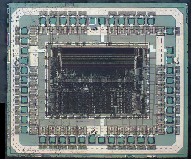
enter image description here

The image is taken from this nice video and features the 1993 800nm version. It shows that, already at that 'crude' size, the minimum area possible, defined by maximum packed pads, sufficient to hold the CPU is reached. Looking closely reveals a comparable large unused area between pads and their pull up/down circuits (*2) and the CPU circuitry. Any further process shrink will therefore not bring savings in area, but only add complications.

It is often forgotten that shrinking adds problems, often quite a lot. A large effort in today's processor design goes into minimizing or mitigating these effects. Heat is the most obvious, but usually not of concern for ancient designs with a few thousand gates. With shrinking size, elements get more sensible for all kinds of distortion, foremost voltage. It is not only for power saving that modern CPUs operate at ridiculously low voltages (like the mentioned 7nm Ryzen with 1.1 to 1.4 Volt): the fine structures would simply fry at higher voltage.

Related to that, shrinking voltage and node size causes parasitic loss to increase. So if low power is a major goal, the smallest available structure size is not a good choice.

Not to mention that rough environments (Military use, Space, etc.) love to kill fine structures on sight, so having bigger ones is a measure of safety.


But There is an Area Where Older CPUs do Shrink Further

The picture changes a bit when not only looking at the CPU itself, but it being a part of a system that gets shrunk together. Imagine a system consisting of

  • Z80 CPU,
  • Z80 DMA,
  • Z80 PIO (maybe more than one)
  • Z80 SIO (")
  • 2 KiB of Boot-ROM
  • 32 KiB of FLASH
  • 2..32 KiB of RAM

To be shrunk into a System on a Chip (SoC). Here each of these additional components is in terms of space requirement comparable, if not higher than the CPU itself. Especially the RAM/FLASH part. Together they come out easy as 20-30 times the CPU alone. Since reduction goes by square, a 25 times larger amount of components will need to be shrunk by 5 to give the same area.

So while it does not make any sense to shrink a 6502 or Z80 below 5-600 nm feature size, a SoC based on such does make sense in 100..120 nm technology, but not below. That is of course only if it doesn't need more pins - as their number is again the limiting factor.


*1 - Being CMOS this was in part compensated by needing about 2.5 times as many gates.

*2 - It nicely shows the difference between power pins, which simply connect to ground and power layer, and signal pins with their drivers. Seeing the drivers already orientated radially (inside and outside of the pads) show that the chip is already optimized for size. In comparison, the original NMOS 6502 (warning, extremely large image) was so large that there was enough space between the pads for many of the drivers to be moved there.

3
  • Comments are not for extended discussion; this conversation has been moved to chat.
    – Chenmunka
    Commented Mar 12, 2021 at 11:54
  • 1
    where do I get my 4mmx4mm chip with 1000 386es on it? Commented Jan 31, 2023 at 10:03
  • 1
    @user253751 Maybe ask Intel - they tried to go that way during the 2010s with the Knights series (Xeon Phi). Given, they didn't use a 386, but older, smaller cores, but 60+ of them. he idea was to exploit massive parallel setups. Didn't work out. While they peaked quite favourable at some very special tasks, over all performance was way below a lower number but more modern cores using the same technology and chips size.
    – Raffzahn
    Commented Jan 31, 2023 at 11:00
26

They're not quite cutting-edge process sizes, but there are current 8051-core micro-controllers that do much better than the 1981 original's 12 MHz on 3.5-μm process silicon. For example, the Cast S8051XC3 has been run at over 600 MHz on a 40 nm process. The core has a few thousand gates, and can attain better than 3 μW/MHz

13

Sometimes...

Well, let's go back to one of the chips that was part of the original home computer revolution - the Zilog Z80. The AMD of the era, the Z80 was binary compatible with the Intel 8080 chip, only better, and could run the CP/M operating system that was the standard before MS-DOS, so your Z80 computer had access to industry standard software like Microsoft BASIC and COBOL, Borland Turbo Pascal, dBASE II, Wordstar, etc...

Zilog is still around and producing the eZ80 - https://en.wikipedia.org/wiki/Zilog_eZ80 - which runs at 50Mhz, and is equivalent to a 150MHz Z80 CPU. Now back in the late 70s/early 80s typical CPUs ran at 1-4MHz. The most common Z80 was a 4MHz version. A 6-8Mhz CPU was considered super fast. 150Mhz would seem insanely quick.

So I'd say at least some old CPUs are still around and have been improved by incorporating modern design and manufacturing ideas. Are they as good as modern CPUs - no, but they are light years beyond what they were in their hey-day.

The eZ80 is marketed as a micro-controller you'd use to open your garage door or trigger a restaurant buzzer nowdays - https://www.zilog.com/index.php?option=com_product&task=product&businessLine=1&id=77&parent_id=77&Itemid=57 - but this was once one of the most popular computer CPUs.

It's still binary compatible with the original Z80 which means some people have done some interesting stuff:

https://hackaday.com/2020/02/23/a-z80-computer-at-the-next-level/

https://www.tindie.com/products/lutherjohnson/makerlisp-ez80-lisp-cpm-computer/

3
  • I don't see any ez80's in that 'ZedRipper'? Commented Mar 10, 2021 at 6:27
  • @Bruce Abbot - You're right. My mistake. I've edited the post to only list ez80 computers. Commented Mar 10, 2021 at 7:21
  • CMOS Z80s (or rather Z88C00*s) are still manufactured in speeds up to 20MHz, which is probably a more reasonable comparison; the eZ80 was a complete redesign retaining only instruction set compatibility AIUI.
    – occipita
    Commented Jan 28, 2023 at 19:39
4

There is nothing preventing someone from doing so.

But an old design is at a major disadvantage, Leading Edge Process will compete with Leading Edge Designs which can demand a much higher premium.

So your 15 year design, with sleepy industrial customers (assuming) will either, but likely both, (1) fail to reduce in cost over time and instead get more costly over time and (2) have long factory lead times and a staccato production schedule as you seek to compete for fab time.

Meanwhile, your “yesterday’s process” fab is sitting idle and offering a discount… However it has a major disadvantage.

Wafer size has changed in parallel to process node changes.

Instead, what manufacturers will typically do, is upgrade a more traditional process node fab to a larger wafer size (standard was say 2″ or 4″, now is 200–300 mm+), this investment seeks to address point (1) from above, getting more product for the same amount of production time while maintaining the process node, fulfilling a market expectation that these parts are cheap, reliable, and will continue to get less expensive and more reliable - like a basic commodity.

1
  • 6
    Further, as an appendix: A die change is seen by many industrial customers (medical, automotive, mfg) as a major component change requiring re-qualification, wheras a production optimization is not as strictly scrutinized. Since older designs that survived the fray will likely have customers with long product life cycles and a conservative outlook on change, it would likely necessitating producing both versions anyway or risk losing market share , thus defeating some of the advantage you might seek.
    – crasic
    Commented Mar 10, 2021 at 20:11
4

If you're willing to stretch the question a bit to include 486 processors (technically a processor "based upon" the 486), then yes.

Such CPUs are embedded within modern Intel chipsets as the CSME (Converged Security and Management Engine), PCH (Platform Controller Hub), and IE (Innovation Engine).

Sources: blackhat slides (a few pages in) and Ron Minnich's talk 'Replace Your Exploit-Ridden Firmware with Linux' (relevant bit starting at 3m41s)

0

There was the Intel Quark microcontroller. It was a 32-bit x86 CPU and its instruction set is the same as a Pentium without MMX. But its production was discontinued in 2019.

2
  • Do you know anything about its internal architecture? I'm guessing it's another "CISC interface, translation layer to RISC core" like Intel's processors from the Pentium Pro onward?
    – AJM
    Commented May 9, 2023 at 14:02
  • Intel Quark is based on the Intel 486 architecture.
    – idspispopd
    Commented Sep 26 at 7:47
-1

Not really.

And there's a good reason other than circuit size relative to IO pad size. Old architectures are simply horrible to work with from a software point of view. You would only do this in case it's a better alternative to updating the software for newer architectures. And that will happen at some point. You're just borrowing time without clearing the technical debt.

A modern cheap ARM-based micro-controller is roughly comparable to a fast 90s PC in performance. But it is far easier to develop low level software for the ARM architecture than some old 386 abomination, let alone anything older.

3
  • 4
    I am sorry, but it seems to be more your opinion than answer, isn't it? Some strong statements ("simply horrible") are very discutable and I am in doubt that's the reason. Commented Mar 12, 2021 at 11:30
  • 3
    This answer doesn't explain why brand new 6502 processors are still being made and sold by the millions - quite a bit older than a 386.
    – Greg H
    Commented Apr 22, 2021 at 6:00
  • The MC68000 and VAX were quite nice to write assembly on.
    – RonJohn
    Commented May 10, 2023 at 13:05

You must log in to answer this question.

Not the answer you're looking for? Browse other questions tagged .