6

Trying to design a Z80 based computer that starts from an EEPROM, loads CP/M to RAM and pages out (switches off) EEPROM to allow CP/M to access full 64K RAM. What is a good way of achieving this ? My current thought process is initially mapping EEPROM to the bottom of TPA (see image), say between 0x1000 to 0x2FFF, use a single JP 0x1000 instruction at 0x0000. Let the code to load CP/M CCP/BDOS and BIOS as well as a small piece of code somewhere on the rest of TPA (say 0x3000) that disables EEPROM and jumps to BDOS. Then jump to 0x3000 when I finish loading everything.

Sounds a bit complicated, is there a more practical way of doing it that you can think of?

Main question is then how to disable EEPROM, all I can think of is a TTL based latch addressed a yet unused portion of TPA to bring CE of EEPROM to high permanently (until the next reset or power cycle). Any recommendations here ?

CPM

9
  • So many choices. If you don't have any i/o mapped devices, then use iorq to set/reset the f/f. A write to the eeprom?
    – Kartman
    Commented Mar 26, 2021 at 10:04
  • 2
    Does this fit retrocomputing? It's more of an electronics question, as you are trying design something new with an old CPU.
    – Justme
    Commented Mar 26, 2021 at 10:35
  • 2
    The traditional method is to use a latched output port to control the ROM 'overlay'. You could also make writes go through to RAM so you can load stuff into it from the ROM Commented Mar 26, 2021 at 10:41
  • 3
    This is a SE.EE question rather than Retrocomputing, although I'm sure people here will run to answer it anyway. To set you going on your own instead: search for the BBC Micro Z80 second processor service manual. That used a ROM on power up which overlaid the first 4 KB of the usual 64 KB of RAM. Reading the first 4 KB got the ROM, all writes went to RAM. When the first instruction above 8000h was executed, the ROM vanished until next power-up, leaving the 64 KB RAM. On power-up, the ROM loaded CP/M then jumped to high RAM to start CP/M and switch out ROM. You can find out more yourself now.
    – TonyM
    Commented Mar 26, 2021 at 11:31
  • I'll check BBC Micro manual, thank you. In terms of relevance I though Z80 and CP/M combination was sufficiently retro and might have been relevant for someone else trying to build the same combination. Please up vote this comment if you think I should remove the post completely.
    – Charles
    Commented Mar 26, 2021 at 12:51

3 Answers 3

9

Preface:

a) This is kind of borderline as it's about generic circuit design. Then again, it's about Z80 and I do see some RC.SE relevant insight that may come from comparing different solutions.

b) There are zillions of ways to do this and it depends on whatever main and side goals there are. The following is my personal take on this issue with an emphasis on pure TTL.


It depends a bit on what the startup code is supposed to allow.

Minimal Setup

If it's strictly about being able to boot from a device, then the most simple configuration is to handle chip select according to read/write access. The goal is to deliver a boot-configuration where all read access is from ROM while writes are directed to RAM and a run-configuration where RAM is enabled for read and write.

The basic setup is like this:

  • A Flip-Flop (half a 7474)

  • Four NAND gates (one 7400)

  • The FF gets reset by system reset

    (Z80 /Reset -> '74 1CLR)

  • The FF clear output is NANDed with inverted write to form ROM /CS

    (Z80 /WR -> '00 1A+1B; '00 1Y -> '00 2A; '74 /1Q -> '00 2B; '00 2Y -> ROM /CS)

  • A15 is NANDed with inverted read to set the FF

    (Z80 /RD -> '00 4A+4B; '00 4Y -> '00 3A; A15 -> '00 3B; '00 3Y -> '74 1PR)

Note, RAM CS generation has been left out as the existing circuitry is unknown. It must not be asserted while ROM CS is active (low). With a bit of thinking the inverting NANDs may be used to incorporate it.

How does it work?

  • After Reset RAM is write only, while ROM is read only (duh).
  • Execution starts at 0000h.
  • All read will come from ROM, Code, as well as data.
  • All write will go to RAM.
  • The boot code can load data from a device (must be in I/O space *1) and write it into RAM.
  • Any read access above 8000h will disable the ROM.
  • When ready it can jump to any address at or above 8000h.
  • Code execution is reading.
  • This will disable the boot ROM and enable read and write (or whatever the usual configuration here is).
  • If the code loaded is to be executed below 8000h, a trampoline function (aka a jump to destination) has to be moved into RAM above 8000h and called.

With just two very basic TTL this is about the minimum possible in classic systems. The main point is to be invisible after use. It will not inflict any constraints on operation and system resources. It does not reserve any resource past its operation.

Of course it could be extended - for example using the set FF to distinguish between power-on reset and later reset (cold vs. warm boot), plus maybe using the second FF to detect two consecutive resets to be interpreted as hard-reset (doing cold boot instead of warm boot). Or have the second FF be cleared by some I/O port, to enable cold boot from software. Possibilities are a lot.

In later years, ca. post 1980, this would be integrated into a PAL, offering many more ways to combine this. So if your system already includes a PAL, then these two chips may easily move inside, while still keeping the main function of a boot time only solution, invisible to any software later on.

And yes, it's of course possible to write software that moves some boot image into RAM without needing RAM itself. The Z80 got plenty of registers to hold pointers and state variables. Even rather complex things can be done that way. Boot code is a great way to hone your skills.


*1 - This is an x80 CPU, so I/O belongs into I/O address space. Even more as the Z80 offers full 64 KiB I/O address space.

9
  • If one has an I/O decode available, one could use something like a 74LS138 and one or more 74LS259 chips to add up to eight groups of eight independently settable output pins which would automatically be cleared on reset. If one wires the Z80's A0-A2 to the '259's A0-D2, and the Z80's A3 to the '259's D, that will allow any bit to be set or cleared with an OUT __,A instruction without having to worry about what's in A.
    – supercat
    Commented Mar 26, 2021 at 20:48
  • While this won't be quite as minimal, it will provide I/O decodes for other devices, and if one uses one register bit to control banking it will leave the other seven available for arbitrary other purposes.
    – supercat
    Commented Mar 26, 2021 at 20:49
  • @supercat As said, there are countless ways to do this. Above had as main goal working with minimal hardware and leaving a zero footprint when done, so no constrains to other system design goals. It must work with any later use case.
    – Raffzahn
    Commented Mar 26, 2021 at 21:09
  • @Raffzahn, thanks again for the explanation. Is there a typo ? 00 1B seems to be left empty, is it going to be /WR -> '00 1A + 1B ?
    – Charles
    Commented Mar 28, 2021 at 9:15
  • And A15 -> 3B on the last step ?
    – Charles
    Commented Mar 28, 2021 at 9:21
2

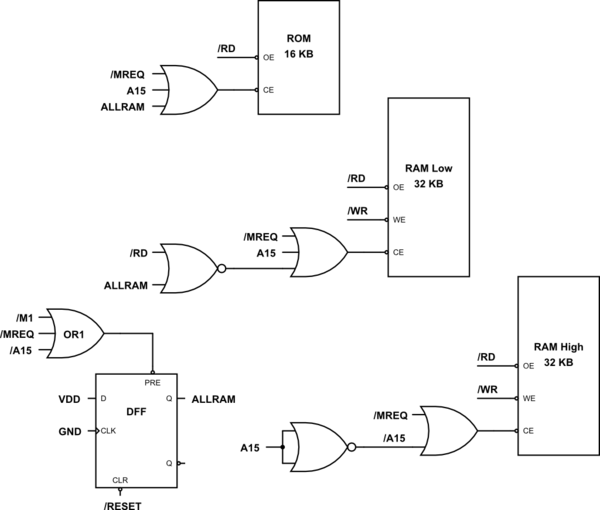
The below circuit shows how it can be done. The principle is taken from the Z80 Second Processor for the BBC Micro and I'm sure the idea was around long before then, these things usually are.

After reset, the Z80 will use a start-up address map. Later, the Z80 will switch to an operating address map.

  • Start-up address map has ROM available (ALLRAM is LOW)
  • Operating address map has no ROM, just RAM (ALLRAM is HIGH).

The start-up address map is:

ADDRESS RANGE    READ                 WRITE
0000..3FFFh      ROM image (16 KB)    RAM Low (first  16 KB)
4000..7FFFh      ROM image (16 KB)    RAM Low (second 16 KB)
8000..FFFFh      RAM High  (32 KB)    RAM High

All Z80 writes go to the 64 KB RAM, so the RAM can be initialised easily. Note that the ROM image appears twice. This harmlessly simplifies the address decoding.

The operating address map is:

ADDRESS RANGE    READ AND WRITE
0000..3FFFh      RAM Low  (32 KB)
8000..FFFFh      RAM High (32 KB)

The start-up address map is in use until the first instruction fetch from the upper 32 KB, which is always RAM.

The system start-up procedure is as follows. After reset, the Z80 will execute from ROM address 0000h. Its ROM software can then follow the following example steps to get into the operating mode and be running CP/M:

Initialise the RAM with CP/M, copied from the ROM or wherever.
Store a 3-byte 'JP startCPM' instruction at 8000..8002h.
Do anything else the ROM needs to, before it vanishes until the next /RESET.
Execute a 'JP 8000h' instruction from ROM.

At the start of the JP instruction byte fetch cycle from 8000h, the D-type Flip-Flop (DFF) output ALLRAM will be preset to HIGH. ALLRAM will stay HIGH until the next /RESET.

schematic

This circuit uses OR and NOR logic gates, to illustrate the mechanisms used. It may well be possible to optimise it into fewer gates. When building one for real, though, you could look at using a CPLD instead (5 V-tolerant or 3V3, depending on your Z80 and memories) such as an XC9500XL part. A CPLD would be cheap and mop up the gates but it just depends what suits you.

1

Dumb approach: wire /IORQ into half a 7474. At boot ldir the bootstrap into the top of RAM, jump to RAM and do any in or out instruction and the ROM vanishes.

Even dumber approach use an R/C circuit, copy the ROM to upper RAM and then spin in high RAM for a second until the ROM vanishes (yes the ROM will randomly page in and out a lot as it passes the threshold voltage but who cares)

Given you have serial on a CP/M system you probably have a spare modem or control like if using an SIO or 16x50 or most other uarts. That can be wired to control the ROM.

Take a look at things like Simple80 for ridiculously low chip count solutions https://www.retrobrewcomputers.org/doku.php?id=builderpages:plasmo:simple80

This uses the SIO to control both the ROM page in/out and the A16 line of the RAM without any glue logic. There's a small error in the design (R16 should go to ground if I remember rightly)

You must log in to answer this question.

Not the answer you're looking for? Browse other questions tagged .