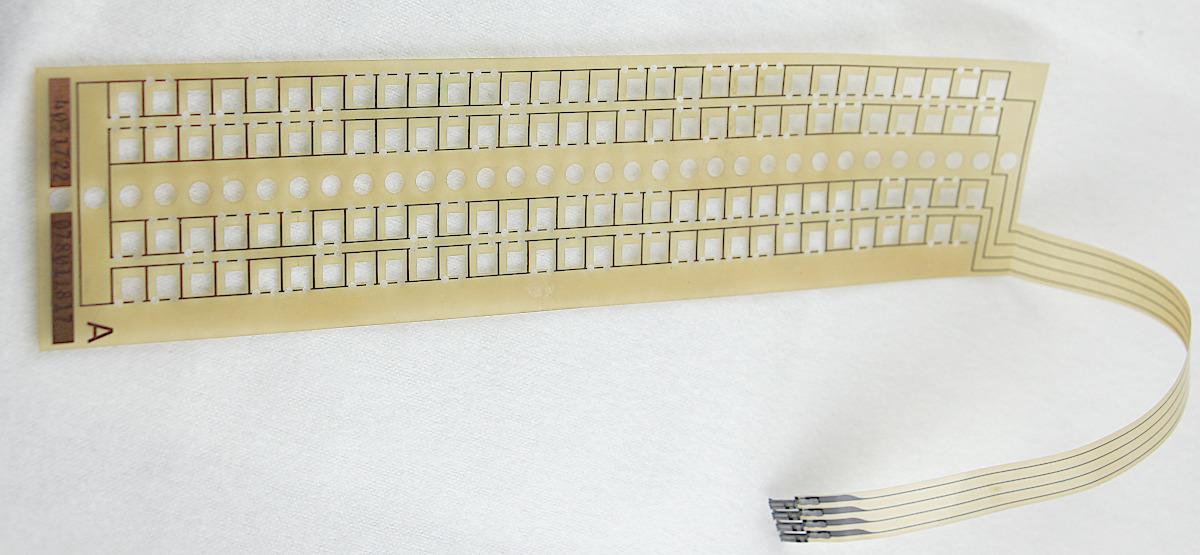
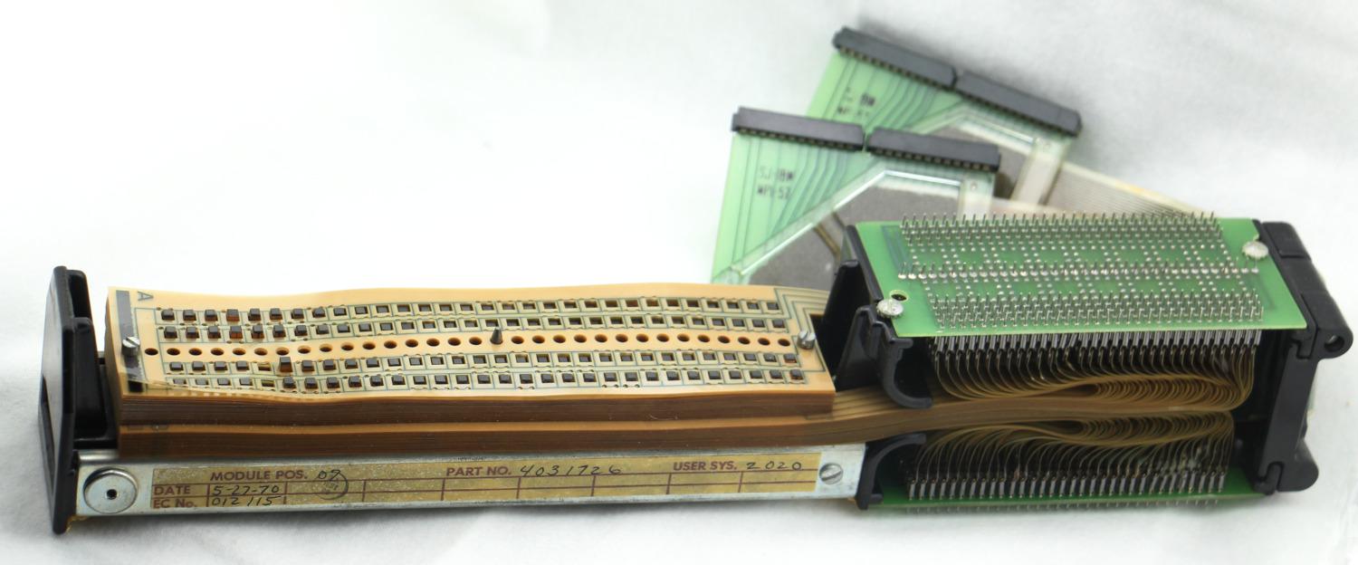
Early on, even fairly small ROM's were quite useful. For example, you could fit a minimal upper-case only font for a terminal into something like 256 bytes. And that's a scale that a human could lay out fairly easily. Fabbing even a small mask ROM has a fairly significant initial cost, and takes quite a bit of time.
But printed circuit boards were a pretty mature technology by the time mask ROM was emerging as a viable option. And if you only needed a grid of something like 64x32 traces, that would not require a huge board. Assuming traces of 0.1" (like pins of DIP sockets and breadboards), a 256 byte "ROM PCB" would only be a bit bigger than 6". Several kilobytes could fit pretty easily in a small backplane.
So, did anybody ever just take the design of a mask ROM and print it directly as traces on a multilayer PCB, rather than in silicon?
edit to add: To be clear, I am not asking about something like a diode array where you have a circuit board full of components, with something like 1 or more components per bit. I am asking about a PCB design where the layout of the traces is the ROM. Such that for example each "stored bit" can be a trace that routes to a power pin vs disconnected or a ground, with no additional per-bit components other than the connectivity of the traces in the PCB. Obviously, I understand you can build discrete logic circuits that work as memory.

