18

I recently came across this question, Why are IC pinouts often so illogical?, which asks:

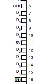
Another example - the Z80's data bus:

Z80 data bus

I mean, that one just makes no sense to me whatsoever. Not only are then in some seemingly random order, but you suddenly get +5V in the middle.

Unfortunately the question is closed and locked, so no answer will ever be forthcoming.

So, why exactly was the power pin placed slap bang in the middle of the data pins? Does anyone who worked on the design know?

Note: I'm not looking for a generic answer as supplied here Why are the pinouts of LPC21xx all over the place? but rather the precise reason given by the Z80 design team, with respect to the design of layer masks. Surely it can't have been that hard to get all of the data lines together, and in the correct order?1


1 What exactly got me to search out the above question was a recent board layout, that I was doing, which incorporated two CD4028 ICs, and I found that the pin out of their data lines is just horrific.

9
  • 1
    A0-A15 are also disjointed, but not nearly so bad. Sometimes you see pinout diagrams for the Z80 where they actually group the bus pins together, then label them with the actual pin number, instead of ordering them by the pin number.
    – Brian H
    Commented Jun 19, 2018 at 14:12
  • 2
    What are you really asking here? Your title asks only about the power pin being in the middle of the data pins (which has an answer that's basically generic to chip design/electrical engineering wrt. power distribution & really isn't anything unusual or special about the Z80; it would be weird if it wasn't the case). However, your question text then implies that you're interested in, but doesn't actually ask, why the order of the data pins is not sequential.
    – Makyen
    Commented Jun 19, 2018 at 15:36
  • 3
    Except for connection to external I/O, it the names of the data lines aren't really so relevant - You can easily reassign D7 to D0 when you are prepared to re-arrange your bits in the ROM a bit. RAM doesn't care at all.
    – tofro
    Commented Jun 19, 2018 at 17:07
  • 2
    Was watching I.T. Crowd recently, and one of the characters goes: "This flipping circuit board, Jen. Some chump has run the data lines right through the power supply. Amateur hour! I've got tears in my eyes!" This question kind of reminded me of that scene.
    – phyrfox
    Commented Jun 19, 2018 at 19:49
  • 1
    "the pin out of their data lines is just horrific" - non-sequential pinouts aren't necessarily a big deal, since on a densely populated board traces often have to take circuitous routes anyway. What's worse is when you have two chips with nicely ordered pinouts, but due to orientation every wire between them has to cross over! Commented Jun 19, 2018 at 22:04

4 Answers 4

21

In addition to Tommy's answer: it is important in designing an IC that uses a lot of power and has large fast variations of power usage (the Z80 is nothing to today's chips in that regard, but it was pushing the boundaries of what could be done in the 70s) that any connection paths that carry a large amount of power are as short as possible, so that impedance caused by variations in power usage don't cause parts of the chip to be run either under or over specified voltage. To this end, connecting VCC and GND is best performed in the middle of the edges (and better still in multiple places -- but the Z80 didn't have enough pins to allow for that). Because of the way the die is aligned in the package, this means that the pins need to be roughly in the middle of the edge (at opposite corners is another approach, which would have the lines landing on the middle of the die on the edges that are mounted across the package width, but then the wires connecting the pins to the die are longer, which is also a potential problem).

2
  • impedance... middle of the edges - thanks, that is something that I hadn't thought of. Commented Jun 19, 2018 at 17:52
  • @Greenonline Impedance isn't the main reason here, as we're talking power supply, not digital lines. Further, as jules explained, pins at the 'end of a chip' also end up in the middle of the die, therefore that makes no difference.
    – Raffzahn
    Commented Jun 20, 2018 at 8:55
19

It's not a complete answer but per Ken Shirriff's hypothesis in "Why the Z-80's data pins are scrambled":

[I]nstead of a single data bus, the Z-80 has a complex data bus that is split into 3 segments. [...] The motivation behind splitting the data bus is to allow the chip to perform activities in parallel. [...] The complex structure of the data buses is closely connected to the ordering of the data pins.

...

The important thing to notice in the diagram above is that everything is packed together as tightly as possible to get the Z-80 to fit on the available silicon. The layout of the Z-80 was done by hand, with each transistor and connection manually positioned. Every possible trick was used to minimize space ...

First, because the Z-80 splits the data bus into multiple segments, only four data lines run to the lower right corner of the chip. And because the Z-80 was very tight for space, running additional lines would be undesirable. Next, the BIT instructions use instruction bits 3, 4, and 5 to select a particular bit. This was motivated by the instruction structure the Z-80 inherited from the 8080. Finally, the Z-80's ALU requires direct access to instruction bits 3, 4, and 5 to select the particular data bit. Putting these factors together, data pins 3, 4, and 5 are constrained to be in the lower right corner of the chip next to the ALU. This forces the data pins to be out of sequence, and that's why the Z-80 has out-of-order data pins.

So you need 3, 4 and 5 in the lower right corner for efficient implementation of BIT, SET and RES. The rest he sort of hand waves away, but one could dare guess that 5v ends up in the middle because its just a lot easier for routing if power arrives in the middle of the die and that the other bits are arranged just as it was convenient to feed the random logic.

8
  • While we're at it, for the 8 bit arithmetic/local operations: ADD, ADC, SUB, AND, OR, XOR etc, bits 3,4 and 5 select which of the operations is to be done. Yet another reason that having them close to the ALU makes sense. Speculating now, but I have often wondered how much the design of the PDP-11 affected the 8080 and hence Z80. The PDP-11 was more often than not programmed in octal, rather than hex, because it makes "more sense" considering the instruction set: bits 0 to 11 inclusive spent a lot of their time as four groups of three, specifying registers and addressing modes. ...
    – dgnuff
    Commented Jun 20, 2018 at 4:35
  • ... In a similar way, on the 8080, bits 0, 1 and 2 spend a fair amount of their time specifying a source "register" ( (hl) is considered a register in this context) And as noted above 3,4 and 5 also spend a lot of time working together.
    – dgnuff
    Commented Jun 20, 2018 at 4:36
  • The die is a square, the pins at the 'end' also end up in the middle.
    – Raffzahn
    Commented Jun 20, 2018 at 8:38
  • @Raffzahn since no human being would ever draw transistors at 45 degrees and the thing is laid out by hand, the corners are not the middle. It's mostly rows.
    – Tommy
    Commented Jun 20, 2018 at 11:17
  • @Tommy No idea what this has to do with 45 degree transistors or layout. Dies are(mostly) square with FOUR sides and the 'corner' pins (like #1 and #21 on a DIP40) end up as well in the middle of an edge - this time the top and bottom edge of the die. You might want think about mabe while taking a look at a random TTL, or for example the 6502 like at visual6502.org
    – Raffzahn
    Commented Jun 20, 2018 at 11:44
5

The Whole Life is a Tradeoff

As always in a real life situation decisions must be made based on contradicting requirements. In this case optimal power supply and easy PCB design are an examples where both are good considerations but hinder each other.

Consideration #1 PCB layout

For simple PCB design it's quite handy if supply power and ground are on opposite 'ends' of a chip (*1). Having one at the 'upper' end (where the mark is) and the other at the lower end (*2) allows a design with a power bar running along one side and a ground one along the other. With a little luck when routing and the usage of rails (*3) it may allow the use of single sided boards with a minimum of discrete wiring (jumpers) - or at least keep a design within two layers. Multiple rows of chips lead to a design with a pair power traces (or rails) running along the middle as seen on many boards.

Consideration #2 Power Supply Quality (Buffering Capacitor)

On the other hand, for a good power supply it's handy to have a right-sized capacitor as close as possible (short routing/wires) to the power supply pins to buffer switching needs. The higher switching frequencies get, the more important this is. Placing power and ground at two adjacent pins would allow adding a capacitor right next to them.

Also, placing both of this pair near the middle of an edge further shortens the wire length, as the internal part of these pins (which in turn are bonded to the die) are here the shortest of all.

Of course routing of power lines will now be rather complex among all the signals. But still manageable - especially when again using rails (*4).

Ok, But Then Why Opposite?

It is desirable to have the same voltage between ground and power across the whole chip area (or as much as possible at least). Unlike simplified assumptions, semiconductors have a rather high resistance, about 10 to 1000 times of copper. Increased by the fact that conductanc is not only defined by the material, but also conducting diameter, power distribution across a chip becomes a serious issue (*5). And no, impedance isn't of much relevance for power supply, as we do not have an alternating voltage (6).

If power was supplied by adjacent pins, the region where these pins are bonded in would enjoy full voltage, while the areas at the other 'end' would get a quite lower supply resulting at least in lower maximum performance if not worse. By placing them on opposite sides of the die, the voltage loss is somewhat compensated over most areas. None gets maximum voltage, but all get about the same (*7) which again is something easing circuit design of the chip.

Putting both on opposite positions (horizontal (*8) or diagonal) is therefore mandatory.

It's important to note that pins using a 'diagonal' layout (like TTL or most other) also end up in the middle of opposite edges of the die - after all, it's square (mostly) and pins are bonded all around.


Bottom Line: Zilog's solution scales better with higher frequency and allows better signal quality, but requires a little more complex PCBs.


*1 - At least for single voltage ones that is.

*2 - I doesn't matter if both are on the same side (left or right).

*3 - These are metal bands with pins in regular intervals like .6 inch or alike. With rails, the routing of power can be eliminated for major parts of a PCB. This was even more important with early automatic routing systems removing a whole dimension of complexity.

*4 - Now standard .6" or 1" rails may not work as well, but it's still better than routing them among all the signals.

*5 - That's also the reason why these huge modern chips have not just one or a few pairs of power pins but sometimes hundreds.

*6 - It is of course relevant if we look at digital lines.

*7 - Yes, there is still variation due to routing and so on, but it's much less than without this consideration.

*8 - The PIO breaks this a bit by using 11/26 instead of 11/29 in favour of keeping all Port B pins adjacent. A little variation doesn't kill the principle.
3

get all of the data lines together, and in the correct order?

Data lines to RAMs have no correct order, they are all equal. The numbering is just a formality but has no real meaning. You can permutate them all you like, still the same data (bytes, words) will come back.

For ROMs (including character generators) it's a different matter, if they are programmed externally. If you swap data lines for reading then in theory you could compensate for that in the programming.

This holds for address lines too, but beware of messing with efficient addressing in pages.

For I/O ports, especially parallel and serial ports, the precise bits matter, but that's nothing that a double sided PCB can't solve.

1
  • As above, I speculate that backwards compatibility with the 8080 explains why the individual data lines have meanings that aren't merely arbitrary — the instruction decoder won't compensate for ROM lines in a different order. But, yeah, you're absolutely right: if you're just building a Z80 machine then connect them up in whatever order is neatest and remember to program the ROM that way around.
    – Tommy
    Commented Jun 20, 2018 at 13:43

You must log in to answer this question.

Not the answer you're looking for? Browse other questions tagged .