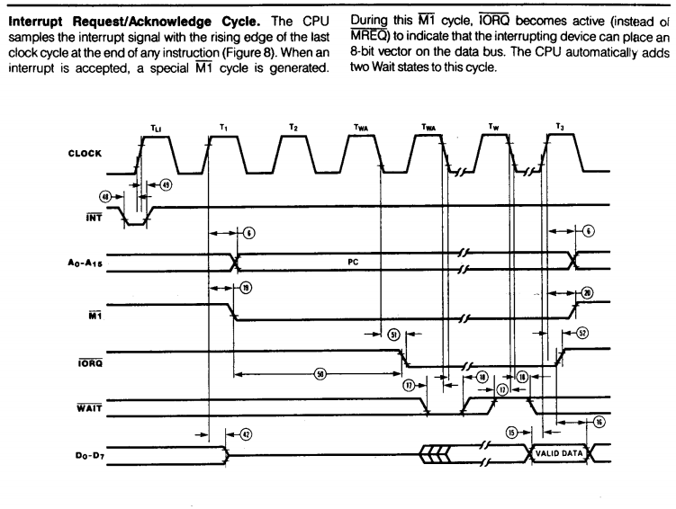
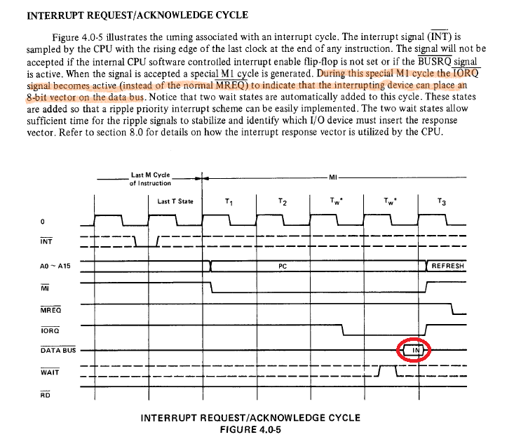
Here's the equivalent diagram from the Z84C00 datasheet (which applies to NMOS Z80s as well as the later CMOS versions), which is a little clearer.

The first thing to notice is that it's actually different: the diagram you show has the bus being released by the device before the CPU deasserts ~IORQ. This is actually wrong: here the timing is explicit, and shows that it must happen after.
This diagram also includes references to the table of timing requirements in the back of the datasheet. (15) indicates that the data must be on the bus at least
TsD(Cr) ns before the positive clock edge - this varies depending on which exact processor you're using, but for a Z84C0004 it's 35ns. (16) indicates that the data must be left on the bus at least ThD(RDr) ns after the IORQ is deasserted, which is 0ns for all processor versions.
There's no specification of how long it can hold on to the bus, because all that's necessary is it stops using it before the next operation starts. In this case, that's slightly more than two clock cycles -- after the acknowledgement cycle the processor continues with the T3 and T4 states of the M1 bus cycle, in which the processor is performing a memory refresh operation which doesn't need the data bus. After that, depending on the interrupt mode, it will either perform a standard M1 instruction fetch cycle or a memory read cycle, both of which give the device until at least 40ns after the negative edge of the clock in the next clock cycle to release the bus before the next request is made.

