8

I have fond memories of programming the 6502, though I never did any hardware hacking with it. I notice that the Altair, with its iconic front panel, was based on the Intel 8080, and from then on, Intel/Zilog and Motorola/MOS Technology ecosystems developed quite separately with limited crossover. The closest thing I know of to a 6502 equivalent of the Altair was the SWTPC which was based on the 6800 and did not have a similar front panel. I'm wondering whether a machine like the Altair could have been just as easily built around the 6502, to what extent this is a matter of technology versus historical contingency.

According to https://en.wikipedia.org/wiki/MOS_Technology_6502

The main change in terms of chip size was the elimination of the three-state from the address bus outputs. This had been included in the 6800 to allow it to work with other chips in direct memory access (DMA) and co-processing roles, at the cost of significant die space. In practice, using such a system required the other devices to be similarly complex, and designers instead tended to use off-chip systems to coordinate such access. The 6502 simply removed this feature, in keeping with its design as an inexpensive controller being used for specific tasks and communicating with simple devices. Peddle suggested that anyone that actually required this style of access could implement it with a single 74158.

That last sounds like hyperbole; a Google search suggests the 74158 was a quad multiplexer, so four of them plus glue logic would've been needed to build a multiplexer for a 16-bit address bus?

But in any case, doesn't the Altair front panel depend on the ability to do exactly what is described, tri-state the CPU in order to take over as a DMA device? Would that be a significant obstacle to building such a system around the 6502 (at least without having to provide extra logic which would tend to negate the cost advantage of the CPU itself)?

9
  • 2
    The Altair front panel is copied from the Mainframes and Minis that also did have such a front panel. So it's definitely not tied to the Z80, and, as you say, with a bit of glue logic if necessary should work for any kind of CPU, 6502 included.
    – dirkt
    Commented Nov 19, 2020 at 12:51
  • 1
    I guess the easiest way would be to map the switches to memory, and then have a simple interrupt routine handle the various requests from the front panel. Commented Nov 19, 2020 at 12:59
  • 2
    @OmarL but that would require a ROM to boot from, and the Altair does not have that. After power-up, there is no program to run, so the front panel is used to load in code before CPU is allowed to execute.
    – Justme
    Commented Nov 19, 2020 at 13:28
  • 1
    @Justme. Well the hypothetical computer would have to be designed rather differently from the Altair I guess, since I believe the 6502 requires a ROM (hint: the interrupt vectors and things are in ROM). And of course, the Altair 680 has a ROM which contains a simple monitor. Commented Nov 19, 2020 at 13:54
  • 3
    @OmarL The point is that "have a simple interrupt routine handle the various requests from the front panel" misses the point of having a front panel. If you already have a "monitor" in ROM, just use a hex-keyboard and a simple display. Yes, of course it could also use many single switches and LEDs, but why bother? A hex-keyboard is cheaper and more convenient. A real front panel, OTOH, doesn't rely on having anything ROM.So the cheapest variant is switches and LEDs.
    – dirkt
    Commented Nov 20, 2020 at 5:29

4 Answers 4

3

TLDR: From knowledge of their general principles of operation, it appears that an Alatir-style front panel could be used with the 6502. However, the devil is always in the details, so to be sure you'd have actually to design and implement a panel and see if you run into any insurmountable technical problems related to subtle details of the 6502's operation.

But in any case, doesn't the Altair front panel depend on the ability to do exactly what is described, tri-state the CPU in order to take over as a DMA device?

No, not in the slightest.

The other two answers here (as of this writing) appear to misunderstand how the Altair front panel works. Being able to tri-state the CPU's address pins (whether via a mechanism internal to the chip or with buffers in front of it) is entirely unnecessary because the front panel never drives the address lines. (The panel does read them to display on the LEDs, but that of course is invisible to the CPU.)

The workings of the Altair front panel were long ago described here on RCSE; this answer quotes a four-paragraph overview of how the panel works and this excellent answer from 比尔盖子 delves into the hardware details, including relevant extracts from the schematics.

The summary of the descriptions above is that the front panel does not drive the address lines itself, it simply instructs the CPU to do so.

  • On pressing the EXAMINE button the front panel ensures that the RAM outputs are not connected to the CPU's data bus, places a JMP opcode on that data bus, and steps the CPU through reading that opcode. It then does that again for two more machine cycles with the values from the address switches. During all of this the address lines are driven by the CPU but essentially ignored by everybody.
  • When the CPU starts the read of the instruction after the JMP, it drives the address bus with the address loaded above, the RAM places the data for that location on its outputs, and the front panel merely reads the address bus and RAM data outputs and displays those values.
  • DEPOSIT-NEXT works similarly except that it has the CPU execute a NOP. The CPU is still driving the address lines and the front panel is sending the data and a write signal to the RAM.

One very important point not addressed in the other answers is that this method of examining an address also has the effect of setting the CPU's program counter. This is quite essential as a front panel directly addressing RAM has no way of telling the CPU where to start execution when you hit the RUN button.

I've not actually tried this out myself on a 6502, but I see no obvious reason that essentially the same setup would not work there, using the RDY line to "halt" the CPU. There may, however, be design subtleties that would cause problems with this; the only way to ensure that there are not would be actually to design and test a front panel.

Regarding the proposition that "the classic solution is [handling it] in software," I've never seen that to be done for Altair-style front panels, only for LED displays and keypads. Those are a vastly different solution, more or less equivalent to having a serial interface and terminal with a machine-language monitor (which was the approach that SWTPC machines took).

But a serial terminal costing more than the computer itself was obviously out of the question for the intended audience of the Altair. I would guess that in January 1975 the front panel was significantly cheaper than even the peripheral interface chips and EPROM or ROM needed to hold a monitor, scan a keypad and drive some 7-segment displays.

3

The Ohio Scientific 300 Trainer is one simple front-panel design for a 6502. It uses the RDY pin to hold the 6502 in a wait state while you're programming it. There are four 7417/7407 hex buffers, and a single 7402 quad NOR, to decouple the CPU address bus from the 6810 SRAM address pins. A whopping 128 bytes of RAM, which has the cost-saving bonus that you don't even need to attach the top 9 address pins to anything!

Downsides: at only $99 you didn't get a "front panel" so much as a bare hand-traced circuit board.

Upsides: you could run it off of four "D" cell batteries for up to 20 hours!


Brad at The Tech Time Traveller has a demo:

1
  • Do you understand what's going on with the 7417 chips bridging the address bus to the LEDs and switches? It looks as though the board is relying upon inherent diodes between the outputs and the inputs when VCC is grounded, but that seems really weird to me.
    – supercat
    Commented Jun 21, 2022 at 22:32
2

But in any case, doesn't the Altair front panel depend on the ability to do exactly what is described, tri-state the CPU in order to take over as a DMA device? Would that be a significant obstacle to building such a system around the 6502 (at least without having to provide extra logic which would tend to negate the cost advantage of the CPU itself)?

Depends on what you want to reach and how.

For simply single stepping, i.e. let the CPU execute a single instruction per step, the classic solution is using the NMI and handle everything else in software, which is in line with the basic 6502 idea of do as much in software. This method was for example used with the KIM. When the SST switch is set, every instruction outside the KIM ROM (*1) fetched (marked by SYNC) will issue a NMI, which is served by the ROM, giving control back to the monitor, allowing any operation to examine/change memory, I/O and as well registers (*2), something not possible by taking over the bus.

Singe cycling, i.e. let the CPU execute one and exactly one clock cycle per step, needs to be done in hardware. Here it's simply about pulling RDY. This works because every cycle of a 6502 is a memory cycle, so pulling RDY will extend that memory access for as many cycles as RDY is active.

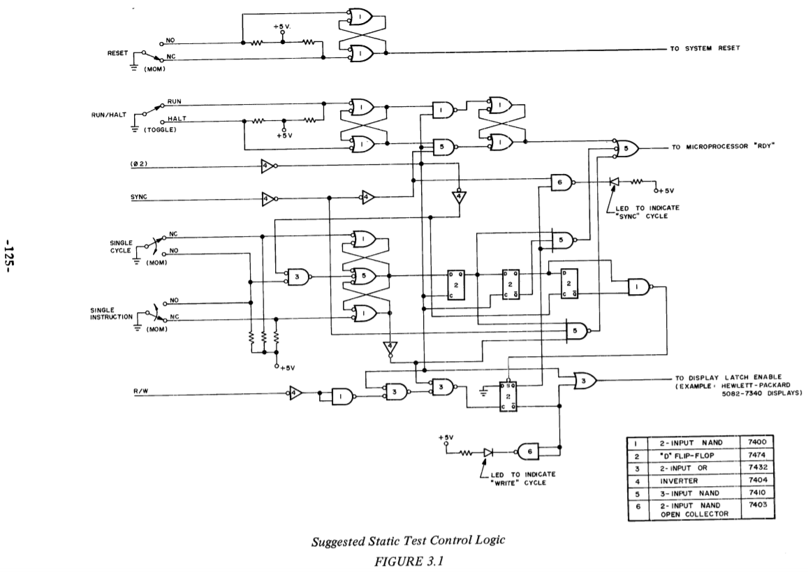
While the basic logic is rather simple, it gets a bit more sophisticated when combining functions. Still, the whole circuitry for single stepping cycles and instructions needs just 6 TTL and fits on a single page of the Hardware Manual :

enter image description here

(Figure 3.1 on p.125 of the January 1976 second edition)

Of course this only lets one static examine bus state and all signals. To be able to read/write memory independent of the CPU, as set of tristate buffers and/or muxes would be needed to take over the bus while the CPU is halted. Plus the usual bunch of switches and LED ofc.

Over all hardware effort would be comparable with Altairs front panel.


*1 - That is only the KIM ROM (6530-002 at $1C000), not the cassette extension (6530-003 at $1800).

13
  • 1
    On the original 6502, doesn't RDY block reads only? And you can't outright stop the clock indefinitely because the registers aren't static.
    – Tommy
    Commented Nov 19, 2020 at 19:46
  • 2
    The stopped clock comment was meant to be a separate comment — I definitely could have phrased that better. Apologies for the ambiguity. But I think you're wrong about RDY. To quote the data sheet: "The Ready input signal allows the user to halt or single cycle the microprocessor on all cycles except write cycles ... [i]f Ready is low during a write cycle, it is ignored until the following read operation.". So I think probably the 6502 couldn't be used with an Altair-style front panel?
    – Tommy
    Commented Nov 19, 2020 at 20:15
  • 2
    @Tommy Oops. You're right. It wasn't until the R65C02 that RDY as well worked for write cycles. It always help to check manual before answering - especially when very sure about a fact :) Sorry. Now, Front panel operation is still possible ... except write cycles will become invisible. I's say adding a latch and a FF could solve that - or using a C02 :))
    – Raffzahn
    Commented Nov 19, 2020 at 20:34
  • 2
    @chthon Single step is when execution gets stopped every instruction, while single cycle is about stopping every clock cycle within an operation.
    – Raffzahn
    Commented Nov 19, 2020 at 20:37
  • 2
    @Raffzahn: Ah yes. From an electronics project in a magazine from around 1978, I actually thought that these things were actually only about single step (project describes such a front-end for a Z80 microcomputer).
    – chthon
    Commented Nov 20, 2020 at 9:14
1

Even without three-state drivers, one could have fairly easily built a computer with an Altair-style front panel by using three-position switches that included a contact for the middle position which would connect the CPU. For the machine to run, the address and data switches would need to be in the middle position to let the CPU drive them. Such a design could be reasonable convenient if it included a couple of hinged levers that would allow groups of eight switches to be switched high or low simultaneously.

Alternatively, a system could use a 25-pole switch to assert READY (freezing program execution with a contact that should break first), disconnect the address and data from the CPU, and connect address to the front panel and data to a ten-pole switch which would disconnect read-enable, connect the data switches, and assert write-enable. While 25-pole switch might seem like a monstrosity, mechanical many-pole switching arrangements used to be somewhat common before the days of electronic control systems. A robust way of doing the switching would be to use a group of roller-actuated microswitches operated by cams, but even contacts sliding on a PC board would likely have worked.

5
  • It is bad to have switches on a CPU bus that can transition at arbitrary times. There is nothing wrong with having unbuffered switches that will only change state at times when the bus is inactive. It might be better to have a separate switch to start and stop the CPU, which was mechanically interlocked with the switch that would connect the address and data buses appropriately, to ensure that the CPU would be halted before the switches operated, but simply having a lever operate some cams, and having an operator refrain from snapping the lever excessively quickly, should suffice.
    – supercat
    Commented Jan 16, 2022 at 21:26
  • Note, btw, that one problem with some unbuffered mechanical switches used for things like selecting printers was that they would connect or disconnect all the wires, including ground, in arbitrary order. When using mechanical switches, it's important to sequence contact openings and closures so that everything will always be in a reasonable state, but if one only moves a switch at a time when electronics guarantee that neither memory-enable nor write-enable will be active, nothing should care. Memory chips don't require that address and/or data wires be in valid states when /CE is high
    – supercat
    Commented Jan 16, 2022 at 21:33
  • It’s not that simple at all. The switches don’t directly drive the bus. They drive a fairly complex controller that interacts with the data and address busses on different ways to set the PC, read and write memory, and single step the CPU. For example, to set PC, the controller has to put JMP on the data bus, run one tick, then put an address on the bus, run one tick, and load the high byte of the address. Then run one more tick. You can’t do that with simple switches.
    – TomXP411
    Commented Jan 17, 2022 at 22:06
  • @TomXP411: Using simple switches, plus a switch to single-step read accesses and a switch to disable memory reads/writes, setting the program counter would require disabling memory reads/writes, clocking in a few EA bytes, then 4C, then the low byte of the desired address and the high byte of the desired address, and then re-connect memory. Hardware to let one set a 16-bit address and hit a button to go there would be more complicated, but wouldn't be necessary to run code on a board that contained a processor, some SRAM, single-step logic, and a bunch of switches, LEDs, and LED drivers.
    – supercat
    Commented Jan 17, 2022 at 22:23
  • @TomXP411: As an alternative minimalist ROMless design, one could build a system with RAM at address zero, a group of nine cam or ten microswitches, and logic so that an access to an address whose MSB was set would assert RDY until the next transition on one of the switches and then use sixteen diodes to couple the value on eight of the other switches onto the data bus. One could then use a pegboard or other such means to load in the sequence of bus reads necessary to store a small boot-loader into RAM and jump to it, followed by the data bytes of a "real" program.
    – supercat
    Commented Jan 17, 2022 at 22:29

You must log in to answer this question.

Not the answer you're looking for? Browse other questions tagged .