13

The 1970s saw a big transition from CPUs built from thousands of discrete components, to CPUs implemented on a single chip, with the occasional use of bit-slice components along the way.

There were, however, some CPUs implemented in a couple of chips. Setting aside coprocessors for floating-point and memory management, one division that was used was a chip for control logic and a second chip for registers and ALU, for example some implementations of the PDP-11: http://simh.trailing-edge.com/semi/f11.html

On the one hand that sounds like a logical division. On the other hand, I'm curious about how it worked in specific.

Late-70s microprocessors tended to be limited by pin count; it was tricky and expensive to go beyond 40 pins, which would quickly be eaten up by address bus, data bus and miscellaneous.

So: the control chip reads an instruction word, which decodes as an instruction to add the contents of a pair of registers. It needs to communicate this to the data chip. How does it do so? The control chip doesn't seem like it would have a bunch of spare pins for that communication, and for that matter nor does the data chip. How do they get around this?
6
  • 3
    There are quite a few non-bitslice multi-chip CPUs besides the F11 (e.g. the Fairchild F8, or the F-14 CADC), and all are restrained by low pin count, and somehow have to distribute everything on multiple chips, and all end up using ways to do so. Are you interested in the F11 specifically? Because I don't think this question has a general answer for all these types of CPUs.
    – dirkt
    Commented Apr 6, 2019 at 8:57
  • To what is the "trickery and expense" with higher pin count associated? Connections to the silicon, pins on the final package, connecting the package to the motherboard? I'd have assumed the first, but on the other hand one answer below cites 80-pin chips.
    – dave
    Commented Apr 6, 2019 at 14:12
  • @dirkt I picked the F11 simply as a representative example. Would be interested in other examples. As far as I can decipher the Wikipedia description, the F8 CPU is on a single chip?
    – rwallace
    Commented Apr 6, 2019 at 16:07
  • @another-dave All of the above. Length of wires from silicon to end pins, mechanics of connecting to the board, standard testing equipment not being designed to go above 40 pins etc. Nothing impossible, to be sure; just tricky and expensive, as I said.
    – rwallace
    Commented Apr 6, 2019 at 16:10
  • 1
    Just wanted to give a shout-out here to the ambitious but failed Intel iAPX-432 - also a two-chip CPU. Bit-aligned variable length instructions - that was easy to decode! Capability-based protection architecture (later seen in the rings/gates of the 80286). IEEE 754 floats!
    – davidbak
    Commented Jun 23, 2020 at 15:58

4 Answers 4

5

Answer for the PDP-11 control and data chips:

In the LSI-WCS user's guide, page 3-4 (page 67 in the PDF) and following describe the division of work between the control chip and the data chip of the PDP-11/03.

The chips themselves are connected by the microinstruction bus (MIB), the data chip is connected to the address and data part of the system bus, while the control chip deals with the control signals of the data bus.

The control chip is responsible for the microlocation address generation and the microinstruction address, it includes a location counter, an incrementer, a return register, and implements conditional and unconditional jumps. It also contains a machine instruction translation register and a translation array.

The data chip has a microinstruction register for the current microinstruction, contains the ALU, the register file both for the "macro" CPU and additional "micro" registers, and the condition code and status flags.

There's lots of details how the microcode actually works, and how the communication between the two chip works in detail, what phases there, etc. and this is all spelled out in the rest of the user's guide.

Again, note that this is specific to the PDP-11. Other multi-chip CPU implementations distributed the work between chips in very different ways.

0
8

The DEC J-11 chipset was a similar design to the F-11, and some pictures are here.

The individual chips were mounted on a chip carrier package, and had more pins (and closer pin spacing) than the package as a whole.

From the pictures, the complete J-11 "CPU" had 60 pins, but the individual chips had about 80 pins each, which seems adequate for the extra interconnections - at least 20, and possibly more if each individual chip doesn't need to access all of the 60 external pins.

The F-11 chips used similar physical packaging. Some of the DEC CPUs had 6 chips mounted on a single carrier.

2
  • 1
    Actually 84 pins per individual chip. There is also documentation on bitsavers for both DC334 and DC335, but I couldn't easily pick internal and external signals. chronworks.com/J11 has a diagram with names for the external pins. It was more common to use multiple control chips for additional microcode, and there were also FP accelerator chips.
    – dirkt
    Commented Apr 6, 2019 at 18:44
  • 1
    @dirkt I didn't have enough fingers and toes to count to 21 along each side of the chips :)
    – alephzero
    Commented Apr 6, 2019 at 19:03
5

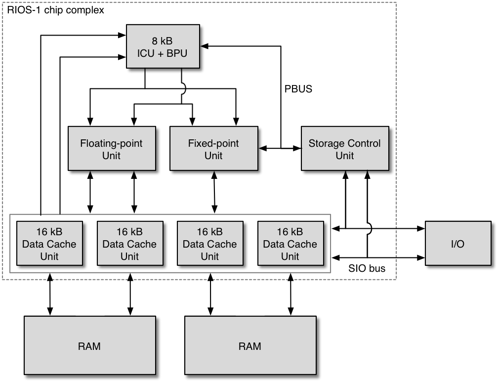
A later example was the original RS/6000 workstation's POWER1 (or RIOS-1) CPU, which was later developed into the PowerPC architecture. Each of the eight VLSI chips contained one major subsystem, along with associated registers and cache; each line in the following diagram is a 32-bit bus.

RIOS-1 chip complex

  1. Instruction Cache Unit (ICU) - L1 I-cache, I-TLB, Program Counter (PC), Link Register (LR), Count Register (CTR), Condition Registers (CR0-7), dispatcher, branch predictor. The ICU executed branch instructions internally, and dispatched other instructions (two per cycle) to the FXU and FPU. The contents of the LR, CTR and CR could also be sent wholesale to one of the FXU's registers.
  2. Fixed Point Unit (FXU) - General Purpose Registers (R0-31), integer execution units, XER, accumulator, D-TLB. Integer and address calculations were carried out here. There was an output to the ICU to update the Condition Registers, upon which a subsequent branch could be predicated, or send a new value to the LR or CTR.
  3. Floating Point Unit (FPU) - Floating Point Registers (FP0-31), double-precision IEEE-754 execution units. As with the FXU, there was an output to the ICU to update a CR.
  4. Storage Control Unit (SCU) - the smallest of the eight chips, this was responsible for arbitrating data transfers both between the other chips and with off-CPU buses.
  5. 4x Data Cache Units (DCUs) - each contained 16KB of the L1 D-cache, as well as ECC logic for workstation-class memory reliability. The RAM was connected directly to these, rather than going through a separate "northbridge" as on the PC.

A ninth chip, known as the I/O Unit, was not formally part of the main CPU chip complex, but could be considered equivalent to the "southbridge" of PC motherboard chipsets.

1
  • Since it is, as you say, a later example, the pin count of the individual chips is much higher (between 184 signal pins for the DCU and 293 for the I/O unit) than 40, so the original problem present in the question isn't an issue for this system.
    – dirkt
    Commented Aug 20, 2019 at 20:45
3

Although the CDP1802 was implemented as a single chip, a preceding version was implemented as two chips. I don't know exactly how functionality was split, but the architecture would have been very amenable to subdivision into two chips--one of which would hold the 4-bit P and X registers along with the sixteen numbered 16-bit registers and the logic to increment and decrement them and the other of which would hold just about everything else. Because all addressing operations are performed using an address specified by one of the registers, only the "registers" chip would need a connection to the system address bus.

If the main CPU gave the address chip a signal indicating when it should be performing an instruction fetch, the address chip could fairly easily watch the instruction stream and know on each cycle which address register should have its value placed on the address bus, which half (if either) should be placed on the data bus, and whether its value should be altered by being incremented or decremented, or having the upper or lower half fetched from the data bus. It could also recognize some instructions to read the P or X registers from either half of the data bus, or output their values on the upper and lower halves of the data bus.

If one observes the bus states on the CDP1802, it actually behaves as though implemented in a fashion somewhat like that. The instructions to move values between the address registers and the data register (accumulator), for example, place the value on the data bus during the transfer. Thus, having the accumulator in one chip but the address registers in the other wouldn't pose a particular problem since the data bus could be used to pass values between the two chips.

8
  • The CDP1802 is like that because it's based on the two-chip CDP1801R and CDP1801U. See en.wikipedia.org/wiki/RCA_1802, and the sources linked to there. Commented Nov 20, 2020 at 7:07
  • 1
    @MichaelGraf: So I guess I not only answered the question of how a two-chip CPU could work, but how one actually did?
    – supercat
    Commented Nov 20, 2020 at 16:39
  • I don't know, to be honest, I just remembered that it was based on an earlier two chip CPU, not how that old CPU worked. But it's very plausible. Commented Nov 20, 2020 at 18:11
  • 1
    @MichaelGraf: Do you like my edit?
    – supercat
    Commented Nov 20, 2020 at 18:48
  • Actually -- according to its Wikipedia page -- the 1802 was based on an earlier design called FRED, which was built from discrete TTL chips.
    – DrSheldon
    Commented Nov 20, 2020 at 22:38

You must log in to answer this question.

Not the answer you're looking for? Browse other questions tagged .